
The design of multiple output power supplies is similar to that of single output supplies. Design considerations and all primary side circuits are the same. However, optimizing the performance of all outputs may require additional design revisions. Determining the right number of turns (voltage centering), the correct wire size (current density) and the optimum winding stack-up (good cross regulation between outputs) can be formidable tasks. This document gives a general overview of what is involved in building successful multiple output Flyback power supplies. For more detailed information on multiple-output power supply design see PI Application Note AN-22.
Feedback information is derived and controlled from the main output of a multi-output Flyback supply. It determines the turns-per-volt (TV) ratio of the transformer.
TV = NSMAIN / [VOMAIN + VDMAIN]
The voltages that appear on the other (auxiliary) windings depend on this TV ratio. Auxiliary winding voltages (VOx) are calculated by dividing the winding’s number of turns (NSx) by the TV ratio and then by subtracting that output rectifier’s forward drop (VDx).
VOx = [NSx / TV] - VDx
Fine-tuning the set-point voltage of auxiliary outputs is easily accomplished. Varying the secondary number of turns (NSx) until the number-of-turns on each auxiliary output are as close as possible the desired output voltage. Remember to use integer values as the transformer cannot be wound with non-integer numbers of turns. In some cases, you can select a low-voltage output as the main winding. This forces the low-voltage output to have an integer number of turns, which should minimize any voltage inaccuracy that might be caused by non-integer rounding errors.
The operating continuous to discontinuous ratio (KP) should be kept as low as possible in multi-output designs. This reduces peak charging (caused by leakage inductance and high peak currents) and improves the cross regulation between the auxiliary outputs. Additionally, output voltage feedback can be taken from the main output alone, or from a combination of outputs. For more information, see the following sections or the Application Note AN-22.
In addition to varying the number of turns, the forward voltage drop (VDx) for each output rectifier can also be modified to achieve better secondary output accuracy. Different types of diodes can also be used to satisfy the peak inverse voltage (PIV) requirements of an output. Output current rating also plays an important role in diode selection to manage diode temperature rise. Additionally, different types of diodes will have varying reverse recovery times (trr) which affects power supply performance.
Schottky rectifiers have a forward drop of approximately 0.5 V and often a low repetitive reverse voltage rating (VRRM) of approximately 60 V or below. Schottky rectifiers are also typically more expensive than other types of diodes but have no reverse recovery time and have very high efficiency due to their low forward voltage.
Fast PN junction diodes typically have a forward voltage drop of approximately 0.7 V and are available with high VRRM ratings, which make them an excellent choice for higher output voltages. Standard PN junction rectifiers with a forward voltage of approximately 1.0 V have very high VRRM ratings, which are common for outputs greater than 22.0 V due to the high PIV seen on these windings caused by the primary to secondary winding ratio.
PI Expert automatically optimizes the type of diode used while PI Xls relies on the user to supply output rectifier information. For a list of commonly used output rectifiers see Table 6 of Application Note AN-43, TOPSwitch-HX.
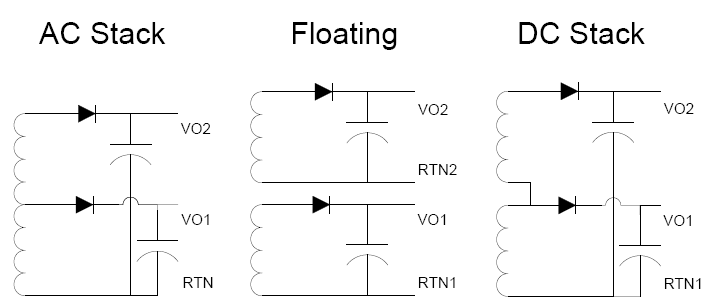
AC-stacked windings improve cross regulation of auxiliary (non-main) outputs. The figure below shows an example of diagrams for both AC/DC-stacked and floating windings.


Multiple output supplies typically use floating or AC-stacked output windings but may also use DC-stacked windings. Floating windings use a separate conductor for each output winding. This provides maximum design flexibility, as you can reference both ends of each winding as desired (each floating secondary winding is galvanically isolated from each other).
AC-stacked and DC-stacked outputs consist of higher voltage outputs on top of lower voltage outputs. These stacked windings are all wound from a common conductor. The start of a set of stacked windings is referenced to a point of common (usually ground) potential to all of the stacked windings. Each stacked winding’s finish is terminated to a transformer bobbin pin after that winding’s required number of turns has been wound onto the bobbin. The next winding in the stack starts on the finish pin of the last winding. Therefore, each greater voltage output’s winding is stacked on top of the lower voltage outputs beneath it. However, independent windings must be used in order to have galvanic isolation from the other windings. Combinations of both independent and stacked windings are also possible.
AC-stacked windings require the lower voltage windings in the stack to carry the cumulative load current of the entire stack. DC-stacked windings require the output diode of the stacked output, in addition to the windings below it, to be specified for the cumulative load current of the entire stack. PI Expert will automatically take these design aspects into account and choose the appropriate wire gauge and output diodes for a given stack configuration. If you wish to stack the outputs of a supply designed using PI Xls, pay attention to the calculated root-mean-squared (RMS) currents of each output (IRMS) and choose the appropriate wire gauges and output diodes. Satisfactory current densities (circular mils per ampere, or CMA) must be maintained within the transformer windings or I2R losses will cause overheating of the transformer and adversely affect its reliability and efficiency. Keep in mind that DC-stacked windings may require additional bobbin pins to accommodate the required termination points.
AC and DC stacking provides for better cross regulation and tracking between the multiple outputs as the load levels on the outputs vary. This is their primary advantage over floating (galvanically isolated) outputs.
In many cases, a combination of floating and stacked windings can be used. See table 3 in the Application Note AN-22 for a comparison of the relative advantages and disadvantages of each winding configuration.
Leakage inductance between the primary and secondary sides of the transformer (and between the various secondary windings) reduces coupling across the isolation barrier and results in less accurate cross regulation of the auxiliary outputs. Transformer optimization involves compromises between performance and output voltage variations over load ranges. Guidelines for the construction of primary windings are provided in the Application Note AN-17 and AN-18 and are valid for multiple output transformers. The following guidelines apply to the optimization of secondary windings:
The winding with the highest current output should be wound closest to the primary winding or windings. This should minimize leakage inductance and the associated voltage spike it produces at switch turn-off.
Outputs requiring the lowest tolerance in output voltage variation should be wound closest to the main (regulated) output. This maximizes the turns-per-volt coupling between the windings and improves the cross regulation of that winding’s output voltage. In some cases, such winding can be interleaved with the main winding.
Fill the width of the bobbin with the turns (increase wire size if necessary) of each secondary winding completely. Consider combining more than one output onto a single layer if this helps to fill that layer. This generally improves the cross regulation of the outputs derived from those windings.
Consider stacking windings that share a common return to improve their cross regulation performance. This can reduce the number of windings required while reducing the leakage inductance and can improve overall solution efficiency.
Minimize PCB trace inductance when laying out high current outputs. Keep PCB trace lengths as short and wide as possible. Keep the area between positive and return (RTN) conductors as short as possible. This should minimize (leakage inductance induced) voltage spikes on these outputs and will improve overall solution efficiency. See Appendix B: Printed Circuit Board Layout Considerations.
Prototype transformers should be constructed and tested to verify their efficiency and regulation characteristics before committing a design to large-scale production.
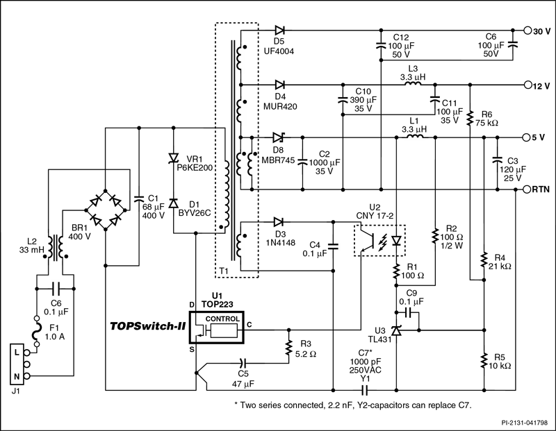
For designs that require low tolerance of output voltage variation on two outputs, shared feedback is an option. The use of a TL431 reference IC lets the designer combine feedback from two outputs simultaneously. This technique gives improved regulation to the chosen auxiliary output while only slightly deteriorating the regulation accuracy of the main output. The diagram in the figure below shows feedback from the 5 V and the 12 V outputs both being combined at the control pin of the reference IC. See page 9 of the Application Note AN-22 for design guidelines related to sharing feedback from more than one output.

A secondary linear regulator can be used to provide tight output voltage tolerance on low power outputs. This has the disadvantage of increased losses and higher cost, but it is simple and can meet tight regulation over a wide load range (dropout voltage must be maintained, which varies according to the linear device). If the auxiliary voltage is proportionally less than that of an existing output, the linear might not require an additional transformer winding (seethe figure below and Application Note AN-22). If a high current output is required and/or the output winding has excessive peak voltages, power dissipation in the linear regulator can be a limiting factor.
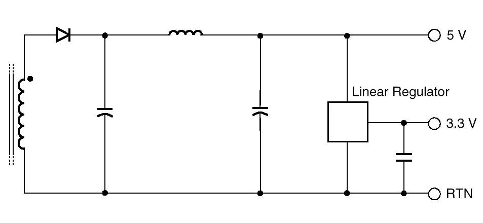

Linear regulator implementation using an existing transformer winding.