TinySwitch-II and TinySwitch-III Design Calculations
The TinySwitch-II design calculations assume worst-case operating conditions. Operation at minimum operating voltage (VMIN), minimum current limit (ILIMITMIN) and minimum switching frequency (FSMIN minus Maximum Jitter) is assumed. The resulting waveform parameter calculation (KP) assumes full power delivery and is based on efficiency (N) and Z-factor (Z) estimates. As is the case with TOPSwitch-GX designs, efficiency and Z-factor are defined at minimum operating voltage.
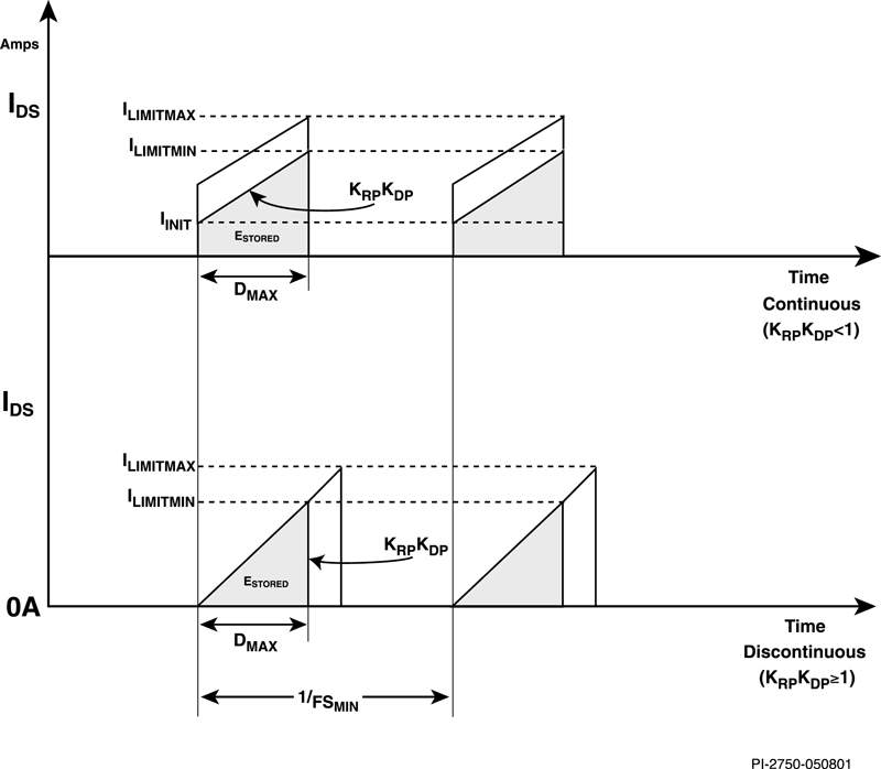
Energy stored in an equivalent transformer is minimal when utilizing a TinySwitch-II exhibiting the minimum current limit (ILIMITMIN) and the minimum switching frequency (FSmin). This is illustrated in Figure 2. The stored transformer energy is equivalent to the grey shaded area under the Drain-Source current (IDS) waveform multiplied by the voltage across the transformer primary windings (i.e., bulk input voltage). This area is labeled ESTORED. These waveforms display both continuous (top) and discontinuous (bottom) operation under steady-state conditions. Actual measurements can vary within cycle skipping mode (see TinySwitch-II Operation).

Figure 2. TinySwitch-II Drain-Source steady-state current waveforms.
Power deliverable by the transformer is equal to the energy stored divided by the total switching period, in seconds (PSTORED = ESTORED / T in units of Watts, and T = 1/FSMIN in units of seconds). The switching period (T) is shown as 1/FSMIN. The power is equal to the familiar term:
PTF = ½ * LPmin * (ILIMITMIN^2 - IINIT^2) * FSMIN.
Termination of the conduction cycle at the maximum current limit (ILIMITMAX) provides extra stored energy. This extra energy is equivalent to the additional non-shaded area shown under the IDS curve in Figure 2. As a result, maximum current limit operation delivers additional energy per cycle. To maintain regulation, TinySwitch-II will disable subsequent conduction cycle(s) (reduced effective switching frequency or cycle skipping) and/or reduce the current limit with a state machine transition (see TinySwitch-II Operation). The amount of overload energy (also called overload power) is, in-part, due to the TinySwitch-II device characteristics. These parameters vary as given in the published device tolerances (see the TNY264-268 data sheet).
Further deviations in overload power can be expected due to transformer primary inductance tolerance (LPmin), which sets the slope of the Drain current curves (see Figure 2). The displayed calculated inductance represents the minimum value required to ensure power delivery with the worst-case TinySwitch-II device characteristics. Primary inductance tolerance can be as high as +/-20%, although +/-10% is typical and depends on transformer manufacturing factors. The Design Results form displays required primary inductance (LPmin) and worst-case TinySwitch-II device characteristics. The designer must work with their transformer vendor to determine the nominal primary inductance and acceptable design tolerance.
As discussed, KP is a calculated value within the TinySwitch-II device family. This calculation is based on device minimum current limit and steady-state duty cycle (DMAX). Figure 2 displays continuous mode (KP<1) and discontinuous mode (KP>=1) operation. Continuous mode occurs when initial current, shown as IINIT, is greater than zero. PI Expert generates applicable warning messages when KP is below feasible limits.
To guarantee acceptable operation with a worst-case transformer design, maximum current limit (ILIMITMAX) is assumed for the following calculations. These calculations assume operation at a reduced effective switching frequency (cycle skipping):
Maximum Flux Density (BM)
AC Flux Density (BAC)
TinySwitch-III design calculations are carried out very similarly to those of TinySwitch-II. However due to the TinySwitch-III's tight I2F tolerances, all calculations performed that involve the minimum current limit or the minimum switching frequency actually use the worst possible case current limit or switching frequency given by the I2F tolerance. This means that due to the tight tolerances of the device, the overall design margin necessary for the power supply can be smaller.
For example, if a part has the lowest possible specified switching frequency it is guaranteed to not have the lowest specified current limit. Instead, the part will have a current limit on the higher side such that it guarantees the minimum specified I2F product. We will use TNY274P for a worked example.
As specified in the data sheet, the I2F product is calculated at both the typical current limit and typical switching frequency.
ILIMIT_TYP = 250 mA
FTYP = 132 kHz
Using the minimum I2F multiplier specified in the data sheet of 0.9 yields.
I2FMIN = 0.9 * ILIMIT_TYP2*FTYP = 7.425 A2 * kHz
Thus, to calculate the worst possible current limit given the data sheet specified minimum switching frequency without including jitter:
FMIN = 124 kHz
ILIM@FMIN = [ (7.425 A2 * kHz) / ( 124 kHz ) ] 1/2 = 0.245 mA
It is shown that a part that is operating with a data sheet minimum switching frequency of 124 kHz will have a current limit no less than 0.245 mA.
Conversely, you can also see that if there is a part with the minimum current limit it is guaranteed to have a switching frequency FS@ILIMIN which is higher than the data sheet minimum switching frequency:
ILIMMIN = 230 mA
Then the worst possible switching frequency (including jitter) for this part would be:
FS@ILIMIN = [ (7.425 A2 * kHz) / ( 230 mA2 ) ] - 4 kHz = 136 kHz
The software will also account for jitter in the worst case, so that the power specified is guaranteed to be delivered.
In conclusion the I2F tolerance on the device helps to reduce system cost by reducing the overall design margin necessary to ensure power delivery and operation of all components within their safe limits.