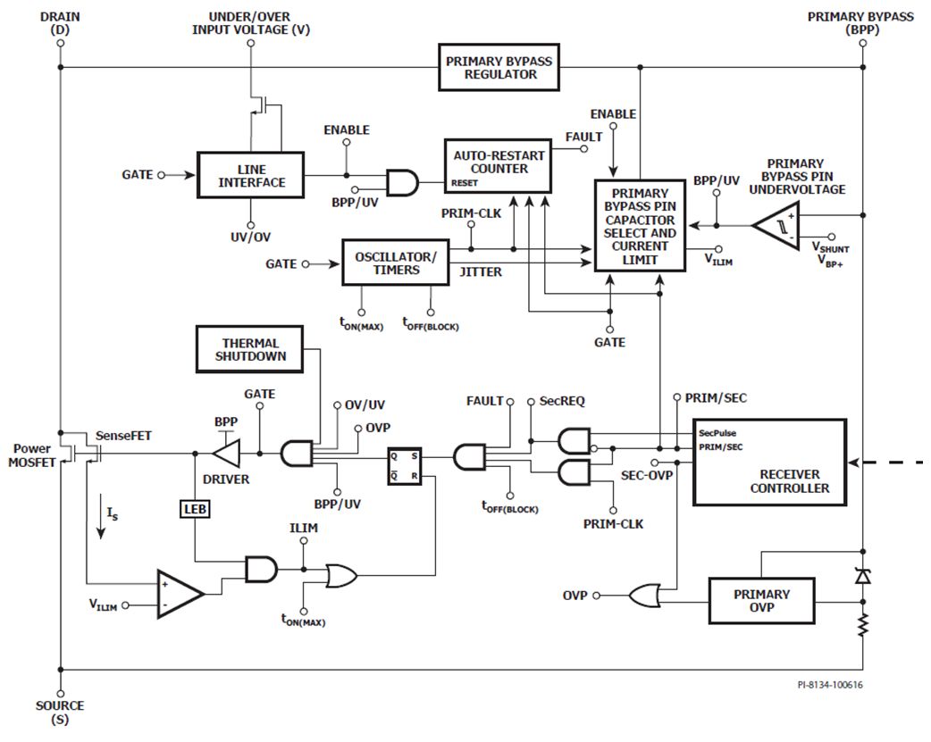
The supply for the primary side internal circuitry of the InnoSwitch-3 controller is connected to the primary bypass pin BPP. An internal regulator charges the bypass capacitor CBPP to 5V. There is also an internal voltage clamp (~5.5V) between the BPP pin and the S pin. See Figure 1 below.

Figure 1
The maximum device current consumption at no load, IS1, is similar for most InnoSwitch3 controllers, whereas the maximum current consumption at full load, IS2, is specific to the device size. Table 1 below shows an example from the InnoSwitch3-EP datasheet.
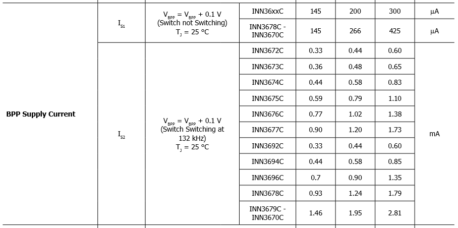
Table 1
It is possible to power the device through the primary bypass regulator, but it should be avoided in normal operation because of heavy power losses and extra heat dissipation in the device. Instead, it is recommended to power the InnoSwitch3 externally from a bias winding connected to the BPP pin.
The following are the primary considerations for the bias winding circuit design:
· Deliver sufficient current into the BPP pin to avoid turning on the primary bypass regulator at all normal operating conditions
· Avoid delivering too much current and triggering the BPP pin internal shutdown down threshold, ISD, at all normal operating conditions
· Minimize the expected power loss on the bias winding at full load and no load
· Minimize the component count
There are two circuits available in PI Expert to power the BPP pin, as shown in Figure 2 (a,b) below. The Simple Resistor circuit is preferable for its low component count. The Linear Regulator circuit is capable of providing tighter control of the BPP current for variable-output voltage designs, which is a typical application for InnoSwitch3-CP and InnoSwitch3-Pro devices.
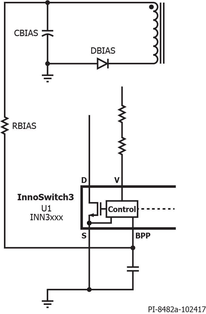
Figure 2a: Simple Resistor
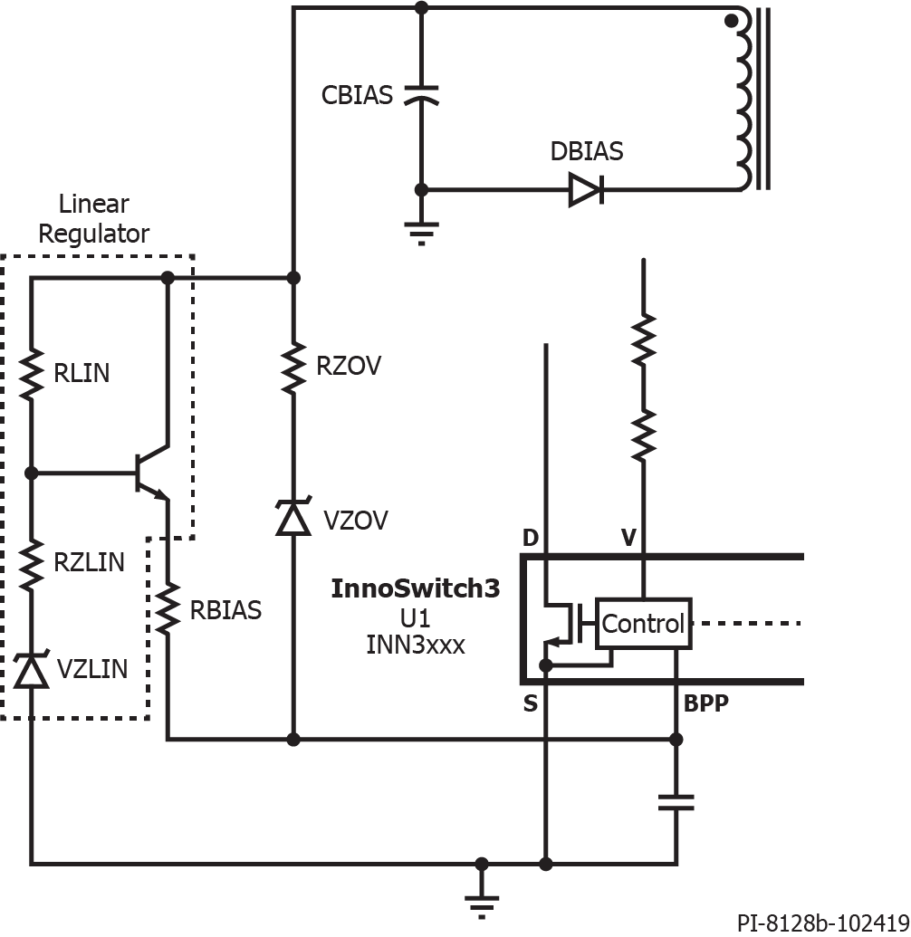
Figure 2b: Linear Regulator
The PI Device Primary Bias Dialog shown in Figure 3 (a,b) below can assist in the design of the circuit. It can be accessed by either selecting RBIAS circuit components from the navigation tree on the left or by right-clicking on a bias component on the schematic and selecting Functional Dialog.
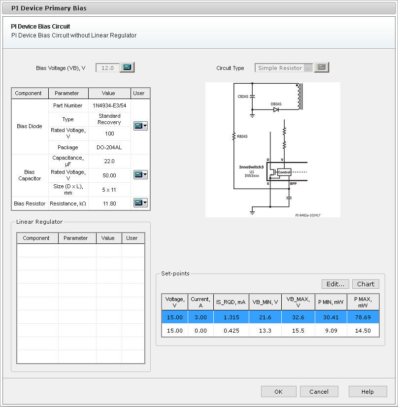
Figure 3a: Primary bias dialog for the simple resistor circuit
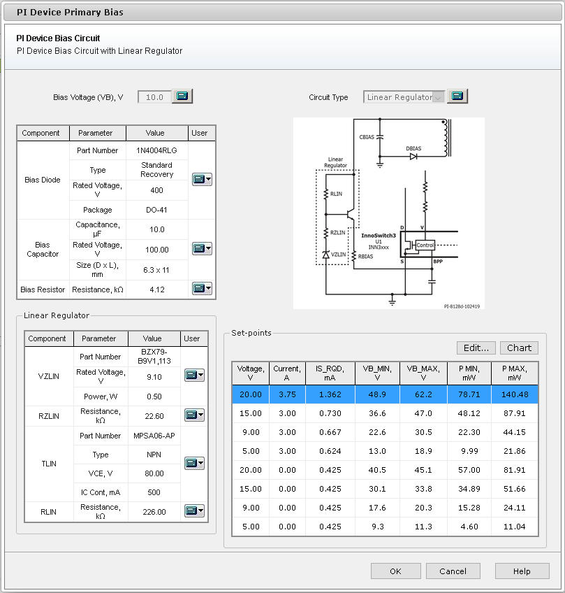
Figure 3b: Primary bias dialog for the linear regulator circuit
In this dialog, Bias Voltage (VB), V sets the target nominal bias voltage for computing the primary bias turns. Circuit Type switches between the two types, but only the Simple Resistor circuit is available for designs that don’t support multiple output voltage levels.
The Set-points table lists parameters at different output conditions of the power converter:
· Voltage – output voltage
· Current – output current. Zero current corresponds to the no-load condition
· IS_RQD – maximum required current consumption of the PI Device
· VB_MIN – minimum voltage on the bias capacitor
· VB_MAX – maximum voltage on the bias capacitor
· P MIN – minimum power consumption of the bias winding
· P MAX – maximum power consumption of the bias winding
IS_RQD is computed from datasheet values and the maximum operating frequency of the converter. VB_MIN and VB_MAX are estimated based on typical designs of this type. It is possible that a better bias circuit can be designed if more accurate values are available from bench measurements. You can adjust IS_RQD, VB_MIN and VB_MAX by clicking Edit, but remember to account for expected variations, because of component tolerances and operating conditions:
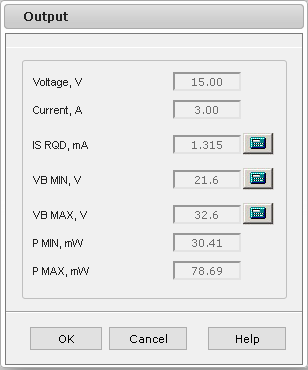
Figure 4: Set-point parameter Edit dialog
You can verify that the circuit provides sufficient current at all operating points by clicking on Charts, as seen in Figure 5. The x-axis lists all of the operating set points, while the y-axis lists the bias current and power consumption ranges. The Min and Max are computed based on VBMIN, VBMAX, VBPP pin voltage tolerances, as well as the tolerances of all bias circuit components. If the minimum is above the required current at all set points, then the primary bypass regulator will not turn on during normal operation.
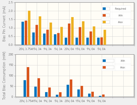
Figure 5: Circuit performance charts
By default, PI Expert selects the components that will minimize the average of Total Bias Consumption over all of the operating set points, including at no load, while making sure that the minimum delivered current stays above the required current. If you are not happy with the selections, you can adjust the components manually by clicking on the ![]() icon next to the component and see the impact on the performance charts.
icon next to the component and see the impact on the performance charts.