 Eq. 1,
“Total Power Supply Losses” in the converter is the sum of the losses in the converter’s main functional blocks: the input stage, PI device, transformer, and output stage. The power loss in each individual block is the total of the losses from the major loss contributors in that block.
For the input stage, major loss contributors for “Total Primary-side Losses” include the bridge rectifier, the input EMI filter and capacitors, safety components such as fuses and VDRs (voltage-dependent resistors), and the primary clamp.
For the PI device, “Total Device Losses” consist primarily of the conduction and switching losses associated with the integrated primary-side switch.
For the transformer, “Total Transformer Losses” consist of copper loss and core loss.
Finally, for the output stage, major loss contributors for “Total Secondary-side Losses” include output rectification devices (diodes and MOSFETS, for example), snubber circuits, and the output EMI filter and capacitors.
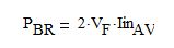
The bridge rectifier loss is calculated as the following:
Eq. 1,
where VF is the bridge rectifier diode forward voltage, and IinAV is the average input current, described by
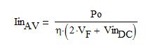 Eq. 2
Eq. 2
Here, η is the efficiency of the converter; Po is the maximum continuous output power; and VinDC is the average DC voltage at the output of the bridge rectifier.
The input filter capacitor power loss PCin is calculated as the following:
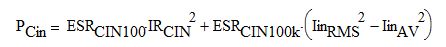 Eq. 3
Eq. 3
Here, ESRCIN100 is the equivalent series resistance of all parallel input filter capacitors at 100Hz at the steady-state operating temperature; similarly, ESRCIN100k is the equivalent series resistance of all parallel input filter capacitors at 100kHz at the steady-state operating temperature. IRCin is the RMS ripple current into the capacitor, and IinRMS is the RMS current in the rectified (DC) input bus.
The power loss in all series EMI and safety components is calculated as a product of the resistance of the components times IinRMS2. The input RMS current is given by the equation:
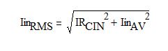 Eq. 4
Eq. 4
Primary clamp losses depend on the type of clamp used: TVS-type, RDC-type, or RDC-Z-type.
For a TVS-type clamp, the loss in the clamp is given by Eq. 5 below:
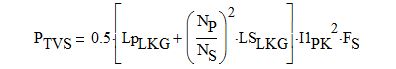 Eq. 5
Eq. 5
Here, LPLKG and LSLKG are the primary and secondary leakage inductance respectively; NP and NS are the primary and secondary number of turns; I1PK is the primary peak current at full power averaged over a mains half-cycle; FS is the switching frequency averaged over a mains cycle.
The loss in an RDC-type primary clamp is calculated as follows:
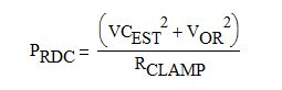 Eq. 6
Eq. 6
Here, VOR is the primary reflected voltage; RCLAMP is the clamp resistor value; VCEST is the estimated voltage across the clamp capacitor CCLAMP as defined by the equation below:
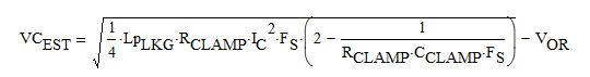 Eq. 7,
where IC is the snubber capacitor peak current.
If an RDC-Z clamp is employed, the power dissipation in the clamp is calculated as below:
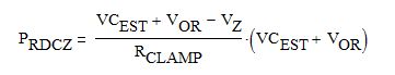 Eq. 8,
where VZ is the Zener voltage.
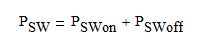
The loss in the PI device is the sum of the conduction loss PCOND and the switching loss PSW in the device:
 Eq. 9
Eq. 9
The conduction loss is calculated as:
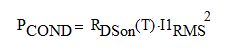 Eq. 10
Here, RDSon(T) is the resistance of the enhanced channel of the primary switch at the operating temperature T, and I1RMS is the primary switch RMS current. The switching loss in the device, PSW, is the sum of the turn-on loss PSWon and the turn-off loss PSWoff.
 Eq. 11
The turn on switching loss estimate incorporates the V2C loss as well as the trans conductance loss as shown by equation Eq. 12 below:
 Eq. 12
Here, COSS is the primary switch output capacitance at the first valley of the idle ring voltage VinDC - VOR; CTEST (≈50pF) is the estimated parasitic capacitance of the transformer reflected to the primary; KRP is the primary current continuity factor (KRP<1 in CCM); TTURNon is the duration of the turn-on transition.
PSWoff is interpolated from experimentally obtained curves of the turn-off energy loss in the primary switch as a function of the peak current I1PK at full power and the voltage supported by the switch after turn off - (VinDC + VOR).
The power loss in the main transformer is calculated as a sum of the copper loss and the core loss. The copper loss is the total of the copper losses in all windings of the transformer. The current waveform for each winding is first resolved in a finite (40 harmonics) Fourier series as follows:
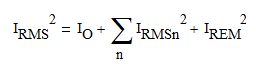 Eq. 13
Where IRMS is the total RMS current in the winding; IRMSn is the RMS value of the nth harmonic current; IREM is the estimated RMS value of the current in the remaining harmonics; and IO is the maximum continuous DC current of the output. Copper effective resistance REFFn is calculated for each harmonic frequency in each winding accounting for skin effect and proximity effect. The total copper loss in the winding PCOPPER is then calculated as:
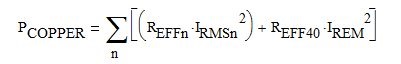 Eq. 14
The core loss is approximated by the following equation:
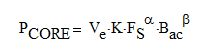 Eq. 15
Where: Ve is the core volume, Bac is the flux density amplitude at full power, K, α and β are frequency-dependent constants. For 10kHz < FS < 100kHz, K = 0.0717, α = 1.72, and β = 2.66.
Because CCM designs operate at KP close to 1, the current at turn-off for all rectification devices is negligible. Hence the turn-off losses in all rectifiers are ignored (PSW.OFF = 0). Consequently, the power loss in any rectifier is calculated as a sum of its conduction loss and its turn-on loss.
 Eq. 16
Output rectification typically utilizes either a MOSFET or a diode.
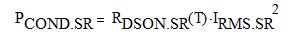
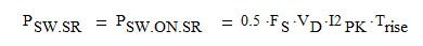
Where a MOSFET is used as a synchronous rectifier, its conduction and turn-on switching loss are given by Eq. 17 and Eq. 18 below:
 Eq. 17
 Eq. 18
Here, RDSON.SR(T) is the resistance of the fully enhanced channel of the SR MOSFET at the operating temperature T; IRMS.SR is the RMS current in the rectified winding (in the channel); VD is the drain voltage supported by the rectifier at the time when the channel current reaches zero; I2PK is the secondary peak current at the beginning of the secondary conduction interval; and Trise is the rise time of the drain current during the turn-on transient.
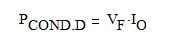
Where diode rectification is employed, the following equations describe the conduction loss PCOND.D and the switching loss PSWON.D in the diode:
 Eq. 19
 Eq. 20
Here, VO is the output voltage, and TSWON is the diode turn-on time.
Simple RC snubbers are employed with all rectifiers. The loss in any snubber PSNUB is given by:
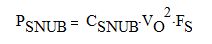 Eq. 21,
where CSNUB is the snubber capacitor value.
The power loss in any output filter capacitor PCOUT is given by the following equation:
 Eq. 22,
where ISRMS is the RMS current in the winding, and ESRCOUT is the ESR of the capacitor. The losses of all output filter capacitors in all outputs are then totaled up.
The loss in the resistive component of any output filter choke is calculated as shown by Eq. 23 below. The losses in all chokes are totaled up.
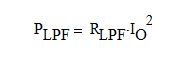 Eq. 23