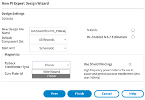
The Magnetics Designer module now supports planar flyback transformer design for InnoSwitch-3. The design methodology is intuitive, highly customizable and provides a Gerber file that can be provided for fabrication.
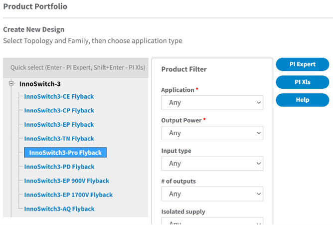
The user can create a planar flyback transformer by selecting ‘Planar’ from the “Flyback Transformer Type” selector in the ‘Design Settings’ dialog box during the design creation wizard.
|
|
The planar magnetic solution generated by PI Expert can be seen in the Magnetics Designer tab. The eight flexible panels contain the whole information about the component.
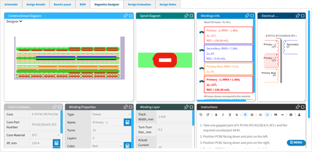
The cross-section of one half of the actual magnetic component assuming that the core’s central pole is on the right side of the drawing is shown in this window. The total height of the winding containing stack is drawn in proportion to the available space.
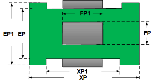
This window contains the information for the magnetic core and currently selected PCB including:
Dimensions – the user can adjust the space available for external connections (pins)
Internal isolation – PCB core and Prepreg’s Type
External isolation – spacers for isolating both sides of the PCB
External pins – dimensions and position
PCB Enclosure Dimensions – the user can adjust the space available for external connections (pins). The space allocated for pins is in the extension XP-XP1 symmetrically on the left and on the right side. Vertically, it could be extended with EP1 above EP dimension.
Contains the currently selected winding information - name, type, connections.
Could be used for adjusting the mechanical and electrical properties of the selected layer.
Displays the actual turns and connections when looking from the top.
Window summarises the currents, turns, resistances, and losses for all winding in the stack.
Represents the windings drawn on an electrical schematic.
Window summarises the steps required for actually creating and finishing the component.
In order to use the Magnetics Designer to successfully customize and finalize the design follow the steps below:
1. Increase or reduce the PCB layers аs needed. This could be achieved via changing the value of the field Layers in Core\Enclosures Properties when the actual PCB is selected. Adding more PCBs is also possible via right mouse click on the drawing.
The engine is trying to present the first result with a good value to money solution of PCB layers’ combination. The final decisions up to the user.
2. If needed, reposition the winding layers via drag and drop on the Constructional Diagram a particular layer to a different place in the stack.
3. If needed, reduce/increase the turns in a layer using the following parameters in the Winding Layer Menu
a. Target Current Density
b. Turn-Turn Minimum Distance
c. Turn-Core Internal Min Distance
d. Turn-Core External Min Distance
e. Copper Thickness, oz
4. Add EMI features – wound shield or screen via right mouse click on the drawing when the selected layer is empty.
5. Add all required pins for external connections via selecting each PCB and using Number of Pins in Core\Enclosure Properties. It is set default to minimum of one but it could be increased as needed. Pins are numbered automatically.
6. Change Pins position, drill holes and copper pad when selecting the pin in Pin Name field and modify the values in:
a. Pin X position, mm (positive values are on the right side from the centre of the Spiral Diagram drawing, negative values are on the left from the centre)
b. Pin Y position, mm (positive values are on the top side from the centre of the Spiral Diagram drawing, negative values are on the bottom from the centre)
c. Pin Pad Diameter, mm and
d. Pin hole, mm.
7. Safety measures implementation.
Actual height of the internal PCB isolations, pins position and distances between copper and core are safety related parameters and should be carefully considered. Three layers of Prepregs and ten FR4 core thickness sizes are provided to achieve the required total layer to layer isolation. All those parameters are in Core\Enclosure Parameters Window and will change dynamically depending on the selected layer in the internal PCB structure.
8. Connect the windings to pins lying in the same PCB. Assign the available pins in Start Pin, End Pin in the Winding Properties. Error will appear if the space required is not enough to trace the winding ends to the pins. Try to swap the pins for the winding ends.
9. Export the files to Gerbers with File/Export../Gerbers command.