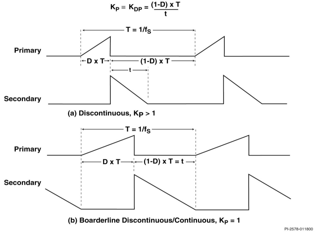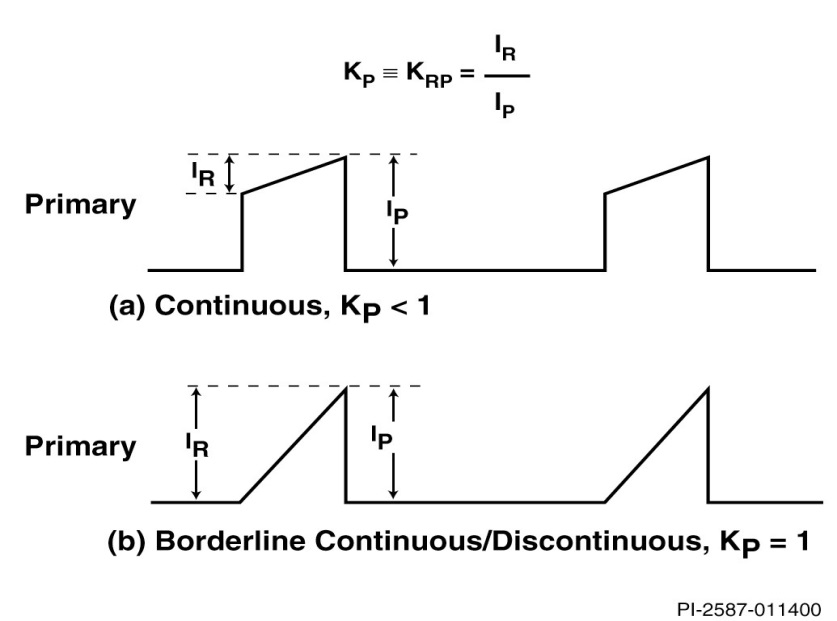
A main consideration for designing a power supply with the InnoSwitch-3 is to minimize the losses on the device and in the system. Those losses include both switching and conduction losses. In order to minimize switching loss, it is good to target a lower frequency of operation. To reduce conduction loss, one should try to minimize ILIM on the device, while still meeting the power delivery requirements with the required margin. Targeting a continuity factor, KP, near one at low line also yields the best thermal performance, though going slightly continuous (in CCM) at low line might be necessary to increase the power for a given PI Device size.
To design with the InnoSwitch-3, one may follow the following step-by-step process:
1. Select the transformer size based on the core area product (AP) or required power at full load.
Calculate the necessary AP of the transformer core and then select a core with higher or equal AP. Alternatively, one can choose the core based on the required power throughput at full load.
2. Choose a device size for the desired output power
First select a device from the applicable product family. Choose a device based on the peak output power of the design. For continuous power, use the “Adapter” column numbers for a fully enclosed type of adapter and the “Open Frame” column numbers, if the power supply is an open-frame type. An example output power table is shown below for the InnoSwitch3-CE family:
Output Power Table
| Product |
230 VAC ±15% |
85-265 VAC |
||
|
Adapter |
Open Frame |
Adapter |
Open Frame |
|
|
INN3162C |
10 W |
12 W |
10 W |
10 W |
|
INN3163C |
12 W |
15 W |
12 W |
12 W |
| INN3164C |
20 W |
25 W |
15 W |
20 W |
|
INN3165C |
26 W |
30 W |
20 W |
25 W |
| INN3166C |
35 W |
40 W |
25 W |
35 W |
| INN3167C |
45 W |
50 W |
40 W |
45 W |
|
INN3168C |
55 W |
65 W |
45 W |
50 W |
If the continuous power exceeds the value given in the power table, use the next largest device. If the continuous power is close to the adapter power levels given in the power table, select a larger device based on the measured thermal performance.
3. Choose the target switching frequency
As an example, one can choose the target switching frequency for the InnoSwitch3-CE family based on the table below:
|
Part Number |
Optimal Frequency at 90 VAC |
|
INN3162C |
80 kHz |
|
INN3163C |
80 kHz |
|
INN3164C |
75 kHz |
|
INN3165C |
75 kHz |
|
INN3166C |
70 kHz |
|
INN3167C |
70 kHz |
|
INN3168C |
65 kHz |
4. Choose VOR
Choose VOR as a compromise between keeping the primary Switch VDS voltage stress as small as possible and keeping the secondary-side MOSFET VDS voltage stress as small as possible. For a high VOR, the primary Switch VDS voltage stress goes up, but the SRFET voltage stress comes down and allows selection of a lower voltage rating MOSFET. Ideally, the chosen VOR for a given output voltage is just high enough so that one does not have to use a higher voltage rating for the SRFET. A lower rating generally allows for lower RDS(ON) for a given power. For example, one can select the VOR such that a 60V SRFET can be comfortably used for a 5V design, 80V for 9V and 12V designs, 100V for a 15V design, and 120V for 20V or higher designs.
5. Select ILIM while calculating KP
For the given device, select between the STD (Standard) and INC (Increased) current limit to satisfy a KP between 0.8 and 1 for a frequency in the range of 60kHz to 85kHz. Keeping KP close to 0.8 at the DC minimum bus voltage (i.e. valley of bus ripple) helps to ensure that most parts of operation can benefit from quasi-resonant switching.