Use the Clamp Components form to modify the clamp circuit suggested by PI Expert when creating a design. You can change the clamp circuit used or choose a different Zener diode or a blocking diode, and modify any of the other clamp components used by selecting them from the Component Library. PI Expert has various clamping circuits available. The software automatically chooses the most appropriate clamp circuit based on the total output power, topology, and feedback mechanism of the supply.
All necessary clamp component values are calculated based on a number of variables. First, the target clamping voltage must be established. For optimum clamp performance, the clamping voltage should be as high as possible, but it is also recommended that a 50 V margin to the maximum Drain to Source breakdown voltage (BVDSS) be maintained. Based on the target clamping voltage appropriate values of the clamp components are selected by the software from the Component Library. You should measure the final clamp design for acceptable thermal performance. Using two series resistors (or zener diodes) to dissipate the power in the clamp circuit is a method that is often used to manage thermal performance.
The following controls are available in the Clamp Components form:
· Clamp Type - Click the calculator icon ![]() on the right of the list box to change the clamp circuit. You can select between RCD Clamp, Zener Clamp, RCDZ and RCD + Zener Clamp based on the device family.
on the right of the list box to change the clamp circuit. You can select between RCD Clamp, Zener Clamp, RCDZ and RCD + Zener Clamp based on the device family.
· You can also edit the Target Clamping Voltage value using the ![]() icon.
icon.
· The icon ![]() indicates that the custom value is specified. Click the
indicates that the custom value is specified. Click the ![]() icon once again to restore the automatically calculated value.
icon once again to restore the automatically calculated value.
The voltage stress on the primary switch of the InnoSwitch-3 and DCDC LYTSwitch-6 is controlled by defining the voltage (VCLAMP_ESTIMATED) above VMAX to which the drain voltage is allowed to reach with the clamp circuit. This entry is user editable. Typically, a 90% voltage de-rating is applied to the device breakdown voltage to determine the default VCLAMP_ESTIMATED. For example, a device with BVDSS = 650 V will have VCLAMP_ESTIMATED close to 210 V so that total voltage stress on the device is less than or equal to 585 V (90% * 650 V). See Figure 1 for details.
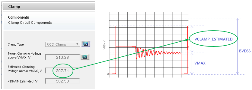
Figure 1: Clamp voltage definitions for InnoSwitch3
For families other than InnoSwitch-3 and DCDC LYTSwitch-6, the voltage stress on the primary switch is controlled by defining the voltage (VCLAMP) above VMAX + VOR to which the drain voltage is allowed to reach with the clamp circuit. This entry is user editable. Typically, VCLAMP = 100 V. See Figure 2 for details.
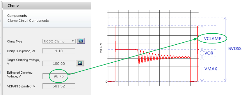
Figure 2: Clamp voltage definitions for families other than InnoSwitch3
Four clamp types are available in PI Expert based. Not all clamp types are available for all families.
RCD
RCD + Zener
Zener
RCDZ
The RCD clamp type is very widely used and highly cost-effective solution to limit the drain voltage of the primary switch. The RCD clamp components (capacitor, parallel resistor, series damping resistor and blocking diode) are selected to ensure that the drain voltage does not exceed the de-rated device breakdown voltage (usually 90% below BVDSS). Once PI Expert has completed the component selection, the estimated voltage stress (VDRAIN_ESTIMATED) on the drain is displayed.
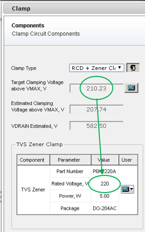
The RCD + Zener clamp circuit consists of the RCD clamp components (discussed previously) with a zener diode connected in parallel with the clamp capacitor. The zener voltage is selected such that it will only conduct if the RCD circuit fails to limit the voltage below its designed operating point. For example, if the user selects an RCD + Zener clamp circuit for InnoSwitch3, a TVS zener rated for 220 V (> 210.23 V as shown in Figure 3) will be selected. Essentially, it is the final protection component in case the RCD clamp fails to operate as expected.
|
Figure 3: RCD + Zener components selection for InnoSwitch3 |
The zener clamp type is the simplest to design and has the lowest part count. Once the user has selected the desired clamping voltage, the appropriate zener is selected to ensure that the user defined voltage stress in not exceeded.
The LinkSwitch-HP family requires proper clamp design to ensure output voltage regulation across load. The RCDZ clamp design ensures that the primary drain-voltage ring decays to a steady-state voltage level before the feedback winding voltage can be sampled. Sampling time increases monotonically from 1.2 ms at no or light load to 2.5 ms at full load.
The designer has the flexibility to pick the individual clamp components instead of defining the clamping voltage – the estimated clamping voltage is re-computed accordingly. Decreasing the clamp capacitance or increasing the clamp parallel resistor has the effect of increasing the clamping voltage and vice-versa. In general, PI Expert will select a standard recovery blocking diode for low power (< 20 W) designs and a fast recovery blocking diode for higher power designs to prevent this diode from overheating.