Bias, Linear Regulator and OVP Circuit
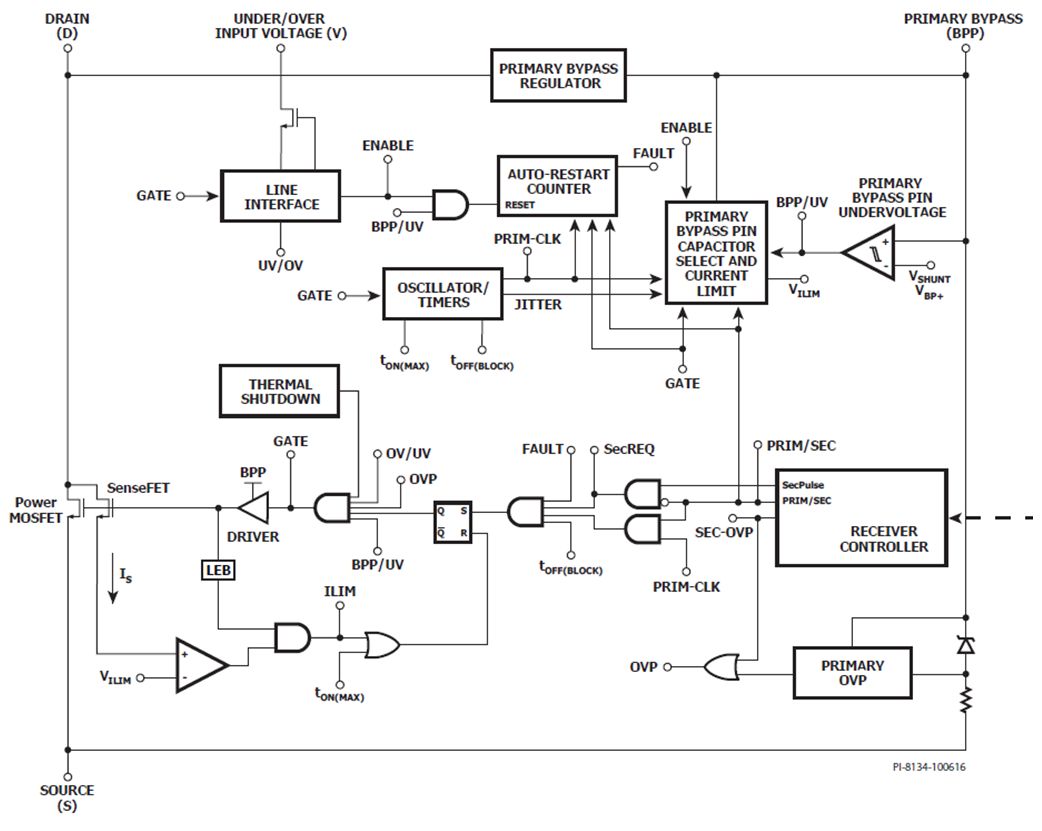
The supply for the primary side internal circuitry of the InnoSwitch-3 controller is connected to the primary bypass pin BPP. An internal regulator charges the bypass capacitor CBPP to 5V. There is also an internal voltage clamp (~5.5V) between the BPP pin and the S pin. See Figure1 below.

Figure1: Controller primary side – block diagram
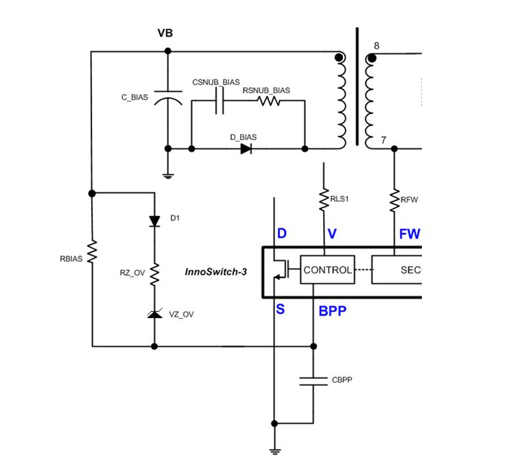
This facilitates powering the InnoSwitch-3 externally from a bias winding as shown in Figure2 below. In the simplest case, the bias voltage VB is connected to the BPP pin via a resistor RBIAS.

Figure2: BPP pin external supply
The bias voltage VB and the current consumption of the BPP pin both increase from IS1 and VBMIN at no load, to IS2 and VBMAX at full load. Note that IS1 is the same for all InnoSwitch-3 controllers, whereas the maximum current consumption IS2 is specific to the device size as shown in Table1 below.

Table1: BPP supply current
The resistance RBIAS needs to be calculated such that it provides to the BPP pin current no less than IS1 at VBMIN and no less them IS2 at VBMAX. Consequently the smaller of the following two values is selected:

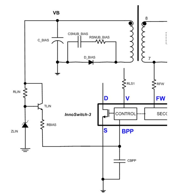
Here, VBPP = 5V, the bypass pin regulator nominal voltage. In programmable output voltage applications (Quick Charge, USB Power Delivery), the output voltage and therefore VB will vary in wide range making the use of a single bias resistor RBIAS unpractical. In such cases, an external linear regulator (LR) is used as shown in Figure3 below. The regulator consists of the components RLIN, TLIN, ZLIN, and RBIAS. Depending on the VB lower limit (VBMIN), the lowest Zener voltage should be used to minimize the losses in ZLIN and RBIAS.

Figure3: BPP external linear regulator.
The BPP pin has a shutdown current threshold ISD = 7.6mA, which can be used to provide basic output over-voltage protection (OVP) by adding resistor RZ_OV and Zener diode VZ_OV in series between VB and the BPP pin (Figure 6). Loss of regulation resulting in an increase in the converter output voltage also causes a corresponding increase in bias voltage VB, driving the Zener diode VZ_OV into breakdown, injecting current in excess of ISD into the BPP pin and causing the controller to shut down. The protection components’ values are calculated as follows:

where
KOVP is the maximum allowed relative increase in output voltage above regulation;
VZ_OV is the Zener voltage;
RZ_OV is the series resistance;
VF is the forward voltage of the diode D1.
Note the following:
1) The OVP threshold (KOVP*VO) established by the above calculations will only be accurate at full load (VBMAX). If regulation is lost at light load (VBMIN), the protection level will be significantly higher. The error is proportional to the difference VBMAX – VBMIN. Therefore the variation of VB with load must be minimized.
2) The actual VB range from VBMIN to VBMAX is difficult to establish analytically. For better accuracy the OVP threshold may have to be set up experimentally on the bench.