
The Tapped buck topology offers the option of a buck converter where the output current is higher than the current limit of the device. The Tapped buck topology is supported in PIXls for the LinkSwitch-II family.
Figure 1 shows the schematic for a tapped buck converter. A power supply using a tapped buck topology operates in a way very similar to one with a buck topology.
Figure 1: The main components of the tapped buck topology
When the switch (S1) turns on (closes), the current linearly increases through the complete inductor (L1, composed of N1 and N2), and through the load. Diode D1 is reverse-biased and so does not conduct during this time. The current continues to ramp up until it reaches the current limit value, which causes the switch to turn off (open).

Figure 2: Switch (S1) closes and current through inductor (L1) linearly increases.
When the switch turns off, the energy in the input section of inductor (L1) couples through to the output (N2) section. The peak current in the output winding steps up by a factor which is equal to the ratio of total inductor turns to the output section turns, keeping the total ampere-turns product constant. This stepped (magnified) current flows out of the output winding, through free-wheeling diode D1, and back through the load. Due to non-ideal coupling between the tapped windings, some of the stored energy does not couple to the output winding.
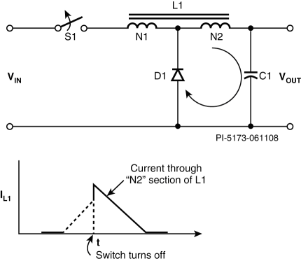
Figure 3: Switch (S1) opens and current through inductor (L1) linearly decreases starting from a larger initial value.
The leakage energy in the input section of L1 causes a voltage spike at turn off. This spike is limited by the intra-winding capacitance of L1. This parasitic capacitance is sufficient to keep the voltage spike from exceeding the BVDSS of the primary Switch.