1 turn
1
1
-
2 turns and more
2
2
0, Return lead
1
1
0, In Lead
2
|
Notification 810 - The value is outside allowed range |
||
|
CATEGORY |
ISSUE / RESULT |
FIX / REFERENCE(S) |
|
Information |
The identified value is less or greater than the limit allowed for that input variable. This range is a practical design limits, or device specification limits, and cannot be altered. |
|
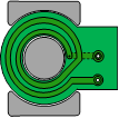
PCB Constructions (vertical / stack dimension)
‘Layer of copper’ is a technologically connected copper material (1oz,2,oz…) to a nonconductive plate (FR4).
The copper is etched to tracks, areas and pads. Some pads or areas could be drilled to provide a hole for components pins. When the internal side of the hole is plated for connecting 2 or more copper layers, they are called VIA.
The PCBs could have ONE or any bigger even number of layers 2, 4, 6, 8, 10, 12...
Planar Magnetics PCBs
In the planar magnetics, mostly the internal layers are used. Creepage and clearance requirements for the internal layers are much smaller than the one for the top and bottom layers.
External pins are exposed externally for the transformer and creepage and clearance requirements apply to the core.
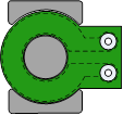
Any other number of a winding turns than ONE, needs minimum of 2 layers to take the lead out.
| Winding TURNS | Min layers | L1 Turns | L2 Turns | Example |
|
1 turn |
1 |
1 |
- |
|
|
2 turns and more |
2 |
2 |
0, Return lead |
|
|
|
1 |
1 |
||
|
|
0, In Lead |
2 |
Table 1 Turns in layer
PCB Constants and internal construction
The PCB Enclosure technology constants are shown here for the user inspection.
Those are the minimum design rule values:
- Minimum Distance Track to Track
- Minimum Distance Track to Core (internal and external to the spiral)
and internal checks for minimum Trace Width.
Those values are function of TT (Track Thickness). Copper ounces used in the layer.
|
Cu |
Copper thickness | Min. Space between Copper Features | Minimum Trace width |
Solder mask thickness |
|
Ounces |
μm |
μm |
mm |
mm |
|
1 |
35 |
89 |
0.09 |
0.08 |
|
2 |
70 |
203 |
0.20 |
0.08 |
|
3 |
105 |
254 |
0.25 |
0.08 |
|
4 |
140 |
0.355 |
0.35 |
0.08 |
|
5 |
175 |
|
0.43 |
0.08 |
|
6 |
210 |
|
0.51 |
0.08 |
|
7 |
245 |
|
0.59 |
0.08 |
|
8 |
280 |
|
0.68 |
0.08 |
|
9 |
315 |
|
0.76 |
0.08 |
|
10 |
350 |
|
0.84 |
0.08 |
Table 2 PCB Internal Properties Dimensions (Technology Tables) position
|
Prepregs |
Thickness |
Final |
|
Types |
μm |
μm |
|
1080 |
75 |
71.25 |
|
2116 |
105 |
99.75 |
|
7628 |
185 |
175.75 |
|
7628R |
216 |
205.2 |
Table 3 Prepreg thickness
|
0.1 |
0.13 |
0.21 |
0.25 |
0.36 |
0.5 |
0.71 |
1 |
1.2 |
1.6 |
2 |
2.4 |
3.2 |
Table 4 FR4 Cores Thickness, mm
|
0.1 |
0.2 |
0.3 |
0.4 |
0.5 |
0.6 |
0.7 |
0.8 |
1 |
1.2 |
1.5 |
1.8 |
2.0 |
2.3 |
2.6 |
3.0 |
3.5 |
Table 5 PADS Drill holes, mm
|
0.1 |
0.2 |
0.3 |
0.4 |
0.5 |
0.6 |
0.7 |
0.8 |
1 |
Table 6 VIA Drill holes, mm
|
0.25 |
0.35 |
0.5 |
Table 7 Metallization Thickness. mm